Attempting a printed circuit board project for the first time can appear intimidating to someone unfamiliar with electronics or has never tried one before. Fortunately, it’s not necessary to be an engineer to design a printed circuit board. Whether you are a hobbyist, inventor, or a student, a step-wise guide to starting the design process can be incredibly helpful. The entire process is often very straightforward with the right guidance and software. Use these seven important steps to guide you through beginning your first printed circuit board design project.
Table of Contents
What is a Printed Circuit Board?
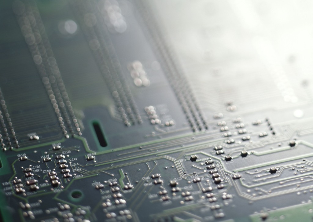
Printed circuit boards, or PCBs, are an essential part of today’s electronics. They feature a compact, organized structure of electrical components. Not only is the PCB a means to contain the elements, but it also connects them. PCBs can be composed of unique materials, various layers and serve a variety of purposes. Whatever type of PCB you intend to design, the preliminary steps will remain the same.
1. Determine Your Budget
Considering printed circuit boards can become very expensive to manufacture, it’s essential to decide on an overall budget for your project. Although you could estimate pcb costs after creating a design, there’s a high risk that you will have to start over from the first step to stay within a reasonable expense window. If you begin your design with a price range in mind, you’ll likely make intentional adjustments to save materials and, ultimately, manufacturing costs. There’s still a chance you will be forced to rework ideas even with an established budget—that’s OK. Use the design process to try various concepts and gain experience. Be sure to include the price of any design software in your budget.
2. Develop a Schematic
Before beginning your PCB design project, you’ll want to decide if you prefer to draw your schematic by hand or use a software program. There are numerous design software options available—be careful to select one tailored to your needs. Should you elect to recreate or modify your PCB project in the future, you will want software that allows you to save the schematic. As a beginner, you likely won’t require advanced tools but know that special features are an option. These capabilities often include simulation or 3D design views, which can be helpful in the process.
Your schematic is the blueprint of your board design. Start with a basic framework that will allow you to check all requirements off your list. You can then group components to save energy or funds. Placement is critical to the functionality and overall success of your PCB design. Begin first with the most fundamental parts, then add and modify around those elements. It’s important to avoid overcrowding or overheating your PCB, so keep that in mind during the schematic stage. The addition of layers can help address this possibility.
3. Compile a List of Components and Materials
Based on your schematic and desired budget, you must gather a list of necessary items with which the manufacturer will create your board. Decide on the materials that you will use and how much will be required of each. Various elements are needed depending on your specific application and industry. Ensure that you’re aware of any standards that your PCB must meet and consider those when compiling materials.
Bill of Materials (BOM)
Your list of raw elements required to assemble the PCB is called a bill of materials, or BOM. This is essentially the recipe for your board—the material guide you will provide the PCB manufacturer with upon completing your design.
Some basic materials you will likely include in your BOM are the following:
- Traces or tracks: the staple of the PCB—most traces are comprised of highly conductive copper.
- Solder mask: a polymer layer that lays over the copper layer of the circuit board. It’s the component that most people picture when they think of the classic green printed circuit board.
- Silkscreen: the silkscreen is the ink printed on the board to identify all components.
- Inductors: stores energy when current flows through it
- Diode: enables one-way current direction while blocking the other direction.
- Resistors: controls the flow of current through a circuit.
- Switches: if closed, a switch will block current; if open, it allows current to flow.
4. Maximize Your PCB Layout
With practice, you will develop strategies to optimize your PCB layout. There are various ways to do so without any strict rules that apply to every design. Much of the applications are learned through trial and error. To make your PCB as efficient as possible, consider these suggestions:
- Adequate spacing: be sure to place components with sufficient distance between to avoid overcrowding. Add layers as needed to sufficiently space components, though note that more layers may mean a more complex board.
- Wiring directions: the orientation of the wiring should alternate between layers. For example, if one layer is configured in a vertical direction, the next layer will feature horizontal wiring.
- Optimal angles: aim to place PCB traces at 45-degree angles. This will also help avoid overcrowding and optimize organization.
Be sure to consider the materials you have chosen for your printed circuit board. Flexibility, rigidity, heat production, and weight distribution are critical factors to be mindful of when developing a layout. This step in the process can be the most frustrating; therefore, it can be useful to step away and view your design with fresh eyes. Avoid hastily finalizing your project layout before optimizing it for maximum efficiency. Taking your time with this step will save you money and energy in the long run.
5. Electrical Rule Checking
If using a PCB design software, you should routinely run diagnostics while developing your schematic and layout. The electrical rules checker will identify any circuit errors. Solutions for each violation may be provided for you depending on the software type. Some issues can be difficult to identify through manual design review; therefore, the software assistance is often instrumental. This ability can be incredibly valuable as it eliminates the possibility of printing a non-functional board.
Common problems identified during the layout process involve:
- Acid traps: this is a tight corner where etchant can become trapped and strip away the copper. Though you can’t officially confirm if your board has any acid traps until after the manufacturing phase, it’s critical to remain mindful of your angles during the layout process to avoid them.
- Electromagnetic problems: your board could be defective if electromagnetic issues arise. Fortunately, you can resolve them during the layout phase. You can aim to increase the board’s ground area and avoid 90-degree angles.
- Pad connections: avoid uneven pad connections during the process by remaining mindful of you pad sizes. Correct pads are essential to the stability of the board foundation therefore resolution of any issues is vital before moving on to production. Consequences of inappropriate pad sizes include solder bridging, incomplete joints, and floating parts.
- Thermal issues: although the material used in a printed circuit board should withstand some heat, overcrowding components can lead to unnecessary overheating. Space elements appropriately and consider the type of materials you included in your BOM.
6. Produce a Gerber File
After settling on a completed design for your printed circuit board, you must generate a Gerber file from which your manufacturer will print the board. Gerber Format is simply the name to which professionals refer to the design files. This standard format is used by manufacturers when producing, building, and buying the actual circuit board. If you used design software to create your board, you could download the Gerber file in its final form.
7. Reach Out to Your PCB Manufacturer
Your PCB manufacturer wants you to get the most out of your PCB design project; therefore, you should contact them with any inquiries or concerns you may have during the process. In-house engineers can offer advice based on years of experience creating PCBs. Not only will it give you valuable insight into the design process, but it will save you valuable money and time. It’s also beneficial for the manufacturer as they also save resources by helping you achieve an efficient design before the manufacturing stage.
Upon completion of your design project, you will want to choose a PCB manufacturer to bring your design to fruition. After presenting your manufacturer with the completed PCB design Gerber files and BOM, they will print your unique circuit board. You can elect to have a prototype board created for testing if you wish. Contact your manufacturer to discuss the best plan of action for your printed circuit board.
Your Printed Circuit Board Design Journey
Numerous resources are available to aid you in your PCB design journey. First, understand the basic steps involved in the design process, then get creative with your custom printed circuit board. Thanks to modern PCB software, a design can be modified or even completely scrapped as many times as necessary in order to produce a functioning board. Don’t hesitate to ask the professional for guidance while you’re first learning PCB design.

Arthur is one of four Co-founders and Engineering Manager of Gerber Labs, an Orange County based engineering startup that is currently rolling out a platform that makes custom printed circuit boards (PCB’s) accessible to electrical engineering students, hobbyists and small businesses.